Cart 0


About IceMOS Superjunction MOSFETs

Since Silicon became the major material for semiconductor devices in 1960's, many researchers have been investigating the limit of Silicon semiconductor performance. In fact, they have created several innovative materials which may potentially exceed Silicon performance, such as various compound semiconductor materials.

Nevertheless Silicon has kept the position as leader of the semiconductor technologies all that long while for the reasons of easiness of manufacturing, high reliability, low cost and continuous innovation.

In the power semiconductor technology world, there was the same event. In principal, breakdown voltage of MOSFET is dominated by carrier concentration of Silicon material and it is directly related to on-resistance of the device. Therefore power device performance is theoretically predicted - it is the so called "Silicon Limit". However "Superjunction" technology broke the "Silicon Limit" and achieved high voltage and low on-resistance, side by side.

IceMOS MEMS MOSFET is the high voltage MOSFET of "Superjunction Technology". By the combination of Silicon MOSFET technology and MEMS process technology, IceMOS provides world-best-in-class performance. Well-known MEMS technology has been developed by unique manufacturing processes in contrast to MOSFET technology which continues progress mainly for smaller dimension. The combination of both technologies encourages advances in extreme performance of MOSFET.


 
IceMOS-Picture1.png
IceMos technology Superjunction MOSFETS

Superjunction MOSFET

superjunction mosfet

Superjunction Features

  • Low On-Resistance

  • Ultra Low Gate Charge

  • High dv/dt Capability

  • High Unclamped Inductive Switching (UIS) capability

  • High peak current capability

  • Increased transconductance performance


Superjunction Applications

  • Power supplies

  • IT hardware : data center, servers, cloud, laptops, tablets

  • Lighting : HID lamp and LED ballast

  • LED TV drivers and power supplies

  • Solar inverters

  • Electric and hybrid cars

  • Electric and hybrid cars


Superjunction Portfolio
A variety of voltages and packages for suitable applications:

  • 600V

  • 650V

  • 700V

  • 730V

  • TO220 (Non-Isolated)

  • TO220 Fullpak (Isolated)

  • TO247

  • D2PAK / TO263

  • DPAK / TO252

  • I2PAK / TO262

  • IPAK / TO251

FastFactsandFigures.png
icemos technology

Global Operations: MOSFET R&D Modeling and Corporate Headquarters in Tempe Arizona (USA), MOSFET R&D and Design Center in Tokyo Japan, Starting Wafer & Substrate Manufacturing in Belfast Northern Ireland.

Over 50% of the 98 worldwide employees have an engineering degree.

Owner of over 80 granted patents, 6 pending, and 14 filed or disclosed.

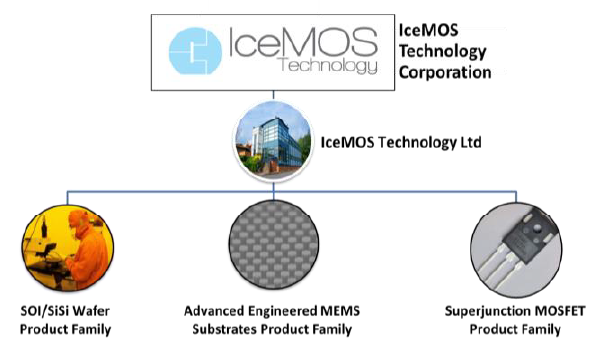
Three Product Families:

• SOI/SiSi Wafers

• Advanced Engineered MEMS Substrates

• Superjunction MOSFETS

Superjunction MOSFET Design -

Less Processing
Lower Cost
High UIS Capability

superjunction mosfet design