
Power Diodes - What Makes Them Different From A Diode?
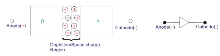
Diodes are the simplest semiconductor device having only two layers, two terminals and one junction. The ordinary signal diodes have a junction formed by p type semiconductorand n type semiconductor, the lead joining p type is called anode and the other side lead joining the n type is called cathode. The figure below depicts the structure of an ordinary diode and its symbol.
Power diodes are also similar to signal diodes but have a little difference in its construction.
In signal diodes the doping level of both P and N sides is same and hence we get a PN junction, but in power diodes we have a junction formed between a heavily doped P+ and a lightly doped N– layer which is epitaxially grown on a heavily doped N+ layer.
The N– layer is the key feature of the power diode which makes it suitable for high power applications. This layer is very lightly doped, almost intrinsic and hence the device is also known as PIN diode, where i stands for intrinsic. As we can see in the figure above that the net charge neutrality of the space charge region is still maintained as was the case in signal diode but the thickness of space charge region is quite high and deeply penetrated into the N– region.
This is due to its light doping concentration, as we know that the thickness of space charge region increases with decrease in doping concentration. This increased thickness of depletion region or the space charge region helps the diode to block larger reverse biased voltage and hence have a greater breakdown voltage. However adding this N– layer significantly increases the ohmic resistance of the diode leading to more heat generation during forward conduction state. Hence power diodes come with various mountings for proper heat dissipation.
Reference Electrical 4U